|
2.9.1 Transistor Models
MOS Transistors
We will show how Analog Insydes can be used to solve practical AC circuit analysis problems by demonstrating the above-mentioned analysis tasks on a number of basic transistor circuits. Although Analog Insydes has built-in device models (see Chapter 4.3), we start with implementing a set of suitable transistor models in order to better understand the modeling language of Analog Insydes. Since bipolar transistor models have already been dealt with to some extent, we begin with a discussion of MOS field-effect transistor models.
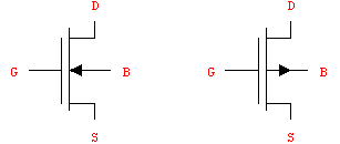
Figure 9.1: NMOS (left) and PMOS (right) transistor
Figure 9.1 shows the schematic representations of an n-channel type (NMOS) and a p-channel type (PMOS) MOSFET on the left-hand side and right-hand side, respectively. The letters D, G, B, and S denote the drain, gate, bulk (substrate), and source connections of the devices. For both NMOS and PMOS transistors, the small-signal operation at DC or low frequencies is characterized by the small-signal equivalent circuit shown in Figure 9.2. The symbol VGS represents the gate-source voltage, which is the main controlling factor for the drain current of the MOSFET, and VBS denotes the bulk-source, or back-gate, voltage. The model parameters of the small-signal equivalent circuits are the transconductance gm, the drain-source conductance GDS and the back-gate transconductance gmb, which is usually, but not always, considerably smaller than gm.
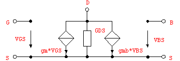
Figure 9.2: Low-frequency small-signal model for MOS transistors
To describe the MOSFET AC operation at higher frequencies more accurately a number of parasitic capacitances are added to the low-frequency model, namely the gate-source and gate-drain capacitances CGS and CGD, and the bulk-source and bulk-drain capacitances CBS and CBD. The resulting high-frequency AC model is displayed in Figure 9.3. For simplicity, we have neglected the ohmic resistances in the drain and source regions which are usually accounted for by two additional resistors in between the physical drain and source connections and the corresponding terminals of the internal MOSFET device.
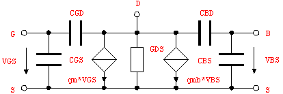
Figure 9.3: High-frequency small-signal model for MOS transistors
Implementation of Small-Signal MOS Transistor Models
For the following calculations we do not need the high-frequency MOSFET equivalent circuit. Therefore, we only implement the low-frequency model at this point. The former will be dealt with later when you have learned more about advanced techniques for associating numerical design-point values with symbolic subcircuit parameters.
In[1]:= <<AnalogInsydes`
In[2]:= lfMOSmodel =
Circuit[
Model[
Name -> MOSFET,
Selector -> LowFrequency,
Scope -> Global,
Ports -> {D, G, S, B},
Parameters -> {gm, gmb, Gds},
Definition ->
Netlist[
{VCG, {G, S, D, S}, gm},
{VCB, {B, S, D, S}, gmb},
{GDS, {D, S}, Gds}
]
]
]
Out[2]= 
To store the model definition in the global subcircuit database we expand the Circuit object using the function ExpandSubcircuits. The contents of the database can be inspected with the command GlobalSubcircuits.
In[3]:= ExpandSubcircuits[lfMOSmodel];
GlobalSubcircuits[]
Out[4]= 
|