|
2.9.3 Device Mismatch
Applying Matching Information
Many analog circuit designs, including our CMOS differential amplifier, rely upon the theoretical assumption that some semiconductor devices are perfectly matched. For instance, the transistors M1 and M2, as well as M3 and M4, must have equal small-signal characteristics to make the differential stage function ideally, i.e. with zero offset voltage and infinite common-mode rejection ratio (CMRR).
For applying matching information Analog Insydes provides the function MatchSymbols. All symbols of a matching group are replaced by a common symbol. In our example, the matching group specification {"$M1", "$M2", "12"} causes all symbols which end with "$M1" or "$M2" to be replaced by a symbol which ends with "12". Thus, gm$M1 and gm$M2 are replaced by gm12, as well as Gds$M1 and Gds$M2 are replaced by Gds12. For the amplifier stage this yields an enormous reduction of the expression size for the differential gain:
In[11]:= dgmatch = Simplify @ MatchSymbols[diffgainDC,
{{"$M1", "$M2", "12"}, {"$M3", "$M4", "34"}}]
Out[12]= 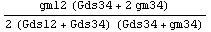
Computing Common-Mode Gains with Mismatch
In practice, however, the matching condition cannot always be fulfilled completely because process tolerances or temperature gradients can cause slight differences in transistor parameters that were originally meant to be identical. The result is a deviation from the nominal circuit behavior which may even be unacceptably large. Therefore, it is necessary to take possible performance degradations due to device mismatch into account during circuit design.
With a symbolic analyzer we can derive formulas which express circuit characteristics in terms of nominal parameter values plus mismatch contributions. In Analog Insydes, accounting for mismatch is simply achieved by assigning the same symbolic element value to two nominally equal components and adding a "delta term" to one of the element values. Two resistors R1 and R2 with the same nominal value R would thus be assigned the values R and R + dR, respectively, where dR represents the mismatch contribution.
To demonstrate this procedure let's examine the influence of device mismatch on the common-mode gain of the CMOS amplifier from Section 2.9.2 (see Figure 9.4). To consider the corresponding mismatch information, we set up a list of replacement rules. Since M1 and M2 should match, both transconductances gm$M1 and gm$M2 are assigned the value gm12. Mismatch is then accounted by adding the delta term dgm12 to the transconductance of gm$M2. Similarly, all other transistor parameter values are expressed in terms of a nominal value plus a mismatch term.
In[12]:= mismatchparams = {
gm$M1 -> gm12, Gds$M1 -> Gds12,
gm$M2 -> gm12 + dgm12, Gds$M2 -> Gds12 + dGds12,
gm$M3 -> gm34, Gds$M3 -> Gds34,
gm$M4 -> gm34 + dgm34, Gds$M4 -> Gds34 + dGds34};
First, we can compute the common-mode gain taking mismatch into account by applying the same unit signal to both input nodes simultaneously, i.e.  and by applying the above defined replacement rules describing the device mismatch: and by applying the above defined replacement rules describing the device mismatch:
In[13]:= cmgmismatch = Together[solcmos /. mismatchparams
/. {V1 -> 1, V2 -> 1, IBIAS -> 0, VDD -> 0}]
Out[14]= 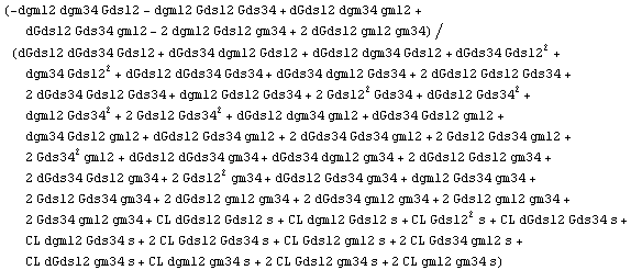
Now, we compute the common-mode gain in the ideal case where all mismatch terms are zero:
In[14]:= Simplify[cmgmismatch
/. {dgm12 -> 0, dGds12 -> 0, dgm34 -> 0, dGds34 -> 0}]
Out[15]= 
Just as expected, for perfectly matching devices the common-mode gain is zero.
In the presence of mismatch terms the common-mode gain is a rather lengthy transfer function whose size makes it hard to read off how the tolerances of individual circuit components contribute to the deviation from the nominal behavior. However, we can find out which mismatch terms have dominant influence by employing symbolic approximation methods (see Chapter 2.8). Below, we choose the design-point values for the MOSFET small-signal parameters gm and Gds taken from the PSpice operating-point simulation. Note that the corresponding data is already included in the above imported Circuit object cmosdiffamp.
Assuming a transistor matching precision of  the delta terms are given by multiplying the nominal values with the delta terms are given by multiplying the nominal values with  . .
In[15]:= dpcmos = {CL -> 1.*10^-13,
gm12 -> 6.*10^-5, dgm12 -> 6.*10^-7,
Gds12 -> 3.*10^-7, dGds12 -> 3.*10^-9,
gm34 -> 6.*10^-5, dgm34 -> 6.*10^-7,
Gds34 -> 8.*10^-7, dGds34 -> 8.*10^-9};
With these design-point values we approximate the expression for the common-mode gain to a coefficient error of  . .
In[16]:= cmgSAG = ApproximateTransferFunction[
cmgmismatch, s, dpcmos, 0.05] // Simplify
Out[17]= 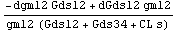
The numerator of the result indicates that the nonideal behavior is largely due to mismatch between M1 and M2. On the other hand, tolerances between M3 and M4 have little impact on common-mode operation.
Computing CMRR
Using the same design point we can also simplify the differential DC gain a bit further, which yields the known approximate gain formula for this amplifier topology:
In[17]:= dgSAG = ApproximateTransferFunction[
dgmatch, s, dpcmos, 0.05] // Simplify
Out[18]= 
Having derived expressions for both the differential and the common-mode gain we can now calculate the common-mode rejection ratio which is defined as the quotient of both quantities. We let  to focus on the DC component only. to focus on the DC component only.
In[18]:= CMRR = (dgSAG / cmgSAG) /. s -> 0
Out[19]= 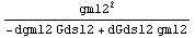
The conclusion that can be drawn from this result is that increasing CMRR requires making the transconductances gm12 of M1 and M2 larger.
|