|
2.9.2 Transfer Functions
A CMOS Differential Amplifier
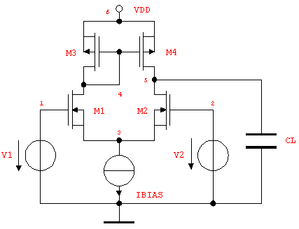
The most basic application of linear symbolic circuit analysis is to compute transfer functions as analytic expressions of the circuit parameters and the Laplace frequency  . For instance, consider the single-ended CMOS differential amplifier stage shown in Figure 9.4 where we might be interested in computing the AC transfer function from the input voltage at node 1 to the output voltage across the load capacitor CL. . For instance, consider the single-ended CMOS differential amplifier stage shown in Figure 9.4 where we might be interested in computing the AC transfer function from the input voltage at node 1 to the output voltage across the load capacitor CL.

Figure 9.4: Single-ended CMOS differential stage
Following, the netlist description of the circuit is not written by hand, but imported via the Analog Insydes command ReadNetlist from already existing simulator files. This function supports the standard application of symbolic analysis which is the extension of a simulation performed with a numerical circuit simulator. By this, a time-consuming and error-prone data conversion by hand is ruled out. In our case we start from a PSpice simulation. Thus, we need to specify the PSpice netlist and output file in the ReadNetlist call, as well as the option setting Simulator -> "PSpice" for applying the simulator-specific interface functionality.
In[4]:= cmosdiffamp = ReadNetlist[
"AnalogInsydes/DemoFiles/CMOSdiffamp.cir",
"AnalogInsydes/DemoFiles/CMOSdiffamp.out",
KeepPrefix -> False, Simulator -> "PSpice"]
Out[5]= 
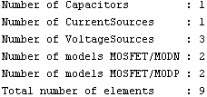
In[5]:= Statistics[cmosdiffamp]

The automatically generated netlist description of the amplifier contains generic model references of the form
 refdes, refdes,  connections connections , ,
Model -> Model[devtype, parset, refdes],
Selector -> Selector[devtype, parset, refdes],
Parameters -> Parameters[devtype, parset, refdes],
 
This allows for an easy exchange of device models and parameter sets for each device or group of devices by means of pattern matching and rewriting. The command CircuitEquations makes use of the above syntax when automatically selecting device models for a specific analysis mode.
Computing the Single-Input to Single-Ended Voltage Gain
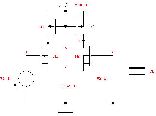
Now, we are ready to analyze the circuit. In order to compute the voltage transfer function from node 1 to node 5 we must first set up a system of circuit equations for the small-signal configuration of the amplifier. This means that all DC sources, namely VDD and IBIAS, are set to zero. Moreover, all signal sources whose contribution is not of interest, i.e. V2, are set to zero as well. The resulting equivalent circuit is shown in Figure 9.5.

Figure 9.5: Differential stage, configuration for small-signal transfer function analysis
In the frequency domain, the relation between a response  , an excitation , an excitation  , and the corresponding transfer function , and the corresponding transfer function  of a linear system is given by the equation of a linear system is given by the equation

Hence, the Laplace transform of the output signal,  , is identical to the transfer function if we let , is identical to the transfer function if we let  : :

Therefore, we can obtain the transfer function of the differential amplifier by applying a unit voltage to the input and computing the output voltage V$5[s] at node 5 because  for for  . .
In the following command line we select the low-frequency small-signal MOSFET model by application of the CircuitEquations option setting DefaultSelector -> LowFrequency (see Section 3.5.1). Additionally, we set up symbolic circuit equations in modified nodal formulation (which is the default for CircuitEquations):
In[6]:= mnacmos = CircuitEquations[cmosdiffamp,
ElementValues -> Symbolic,
DefaultSelector -> LowFrequency]
Out[7]= 
Next, we solve the MNA equations for V$5 using the function Solve:
In[7]:= solcmos = V$5 /. First[Solve[mnacmos, V$5]]
Out[8]= 
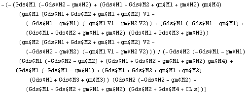
Finally, we apply a list of replacement rules to replace the values of the DC sources and V2 by zero, set the input voltage V1 to  , and rewrite the desired transfer function into canonical sum-of-products form using the Mathematica function Together: , and rewrite the desired transfer function into canonical sum-of-products form using the Mathematica function Together:
In[8]:= tfcmos = Together[
solcmos /. {V1 -> 1, V2 -> 0, IBIAS -> 0, VDD -> 0}]
Out[9]= 
Note that alternatively one could use the functions UpdateDesignPoint and ApplyDesignPoint to modify or insert design-point values.
Computing Differential Gains
Similarly, we can compute the differential gain of the amplifier by splitting up the input signal into two equal parts with opposite phase, i.e.  and and  . .
In[9]:= diffgain = Together[
solcmos /. {V1 -> 1/2, V2 -> -1/2, IBIAS -> 0, VDD -> 0}]
Out[10]= 
From this formula, the DC gain can be obtained by setting the complex Laplace frequency  : :
In[10]:= diffgainDC = diffgain /. s -> 0
Out[11]= 
|