Thermal Contact
Introduction
Thermal management is of crucial importance in modern-day electronics devices. Specifically, inadequate dissipation of the heat generated directly impacts the performance and durability of such devices. Furthermore, enclosures for electronic devices play a crucial role in facilitating the efficient transfer of heat to the surrounding environment. In many cases, the electronic device is connected to a heat sink. And, particularly, efficiency in the energy transfer from the device to the heat sink is of crucial importance in this process. When the device and the heat sink are brought together, a small region between the two objects, known as a thermal contact (TC), is formed. The TC can have a noticeable impact in heat management, since it can directly affect the efficiency with which heat is transferred from the device to the heat sink.
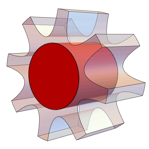
In this notebook, the heat management of a central processing unit (CPU) attached to a heat sink is modeled, based on the work by Grujicic et al. [Grujicic, 2005]. In particular,the effect of the TC on the maximum temperature the CPU reaches is investigated. For instance, see Figure 1.
Figure 1: The schematic shows a cylindrical silicon CPU in red, surrounded by an aluminum heat sink.
The contact between the silicon CPU and the aluminum heat sink will be modeled by a small gap with appropriate material parameters.
Geometry
To keep things simple, 1/8 of the geometry will be modeled in 2D. There is a silicon region for the CPU, a gap to model the thermal contact and a third region for the aluminum heat sink.
The offset specifies the width of the gap.
The "AngularDeflection" option has been used to get a more refined mesh. Also, note that the boundary mesh created is a three-dimensional object. For that reason, it will be projected into two dimensions.
Model
Define the convective boundary condition on boundaries with ElementMarker equal to ![]() and
and ![]() with specified heat transfer coefficient and ambient temperature.
with specified heat transfer coefficient and ambient temperature.
Define the symmetry boundary condition on boundaries with ElementMarker equal to ![]() and
and ![]() .
.
The next plot visualizes the temperature along a line connecting the origin to the outermost boundary. One possible choice is the radial line defined by the angle ![]() with respect to the
with respect to the ![]() axis.
axis.
Modeling the thermal contact with a gap is effectively creating a discontinuity at the gap, which is the expected behavior.
References
1. Grujicic, M., Zhao, C. L. and Dusel, E. C. (2005). "The Effect of Thermal Contact Resistance on Heat Management in the Electronic Packaging." Applied Surface Science, 246(1–3), 290–302. https://doi.org/10.1016/j.apsusc.2004.11.030.
